Published On Jan 18, 2021
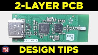
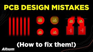
A look at common PCB design mistakes (trace widths, clearances, via placement, copper fills, and silkscreen) and how to improve your PCB designs with some simple rules and ideas. Featuring a mixed-signal PCB from JLCPCB (6-layers) that we will be designing together in the upcoming PCB design course!
Visit https://jlcpcb.com/RHS for $2 for five 2-layer PCBs and $5 for five 4-layer PCBs.
Course survey: https://docs.google.com/forms/d/e/1FA...
PCB Design Toolkit: https://saturnpcb.com/pcb_toolkit/
Git: https://github.com/pms67
Rick Hartley Video: • [LIVE] How to Achieve Proper Groundin...
If you're enjoying my content, please consider becoming a patron:
/ phils94
[TIMESTAMPS]
00:00 Introduction
00:26 JLCPCB
00:55 PCB Design Course
01:15 Saturn PCB Design Toolkit
01:19 #1 Trace Width
03:18 #2 Clearance
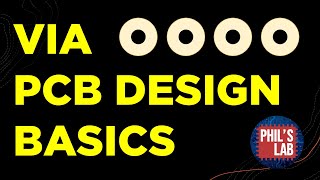
05:21 #3 Via Placement
07:06 #4 Copper Fills
08:32 #5 Silkscreen
ID: QIBvbJtYjWuHiTG0uCoK