Published On Oct 27, 2022
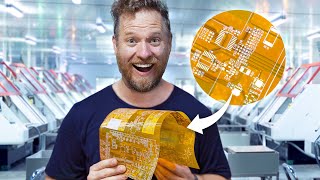
Everything important you need to know when designing FLEX PCBs. Explained by Ata Syed
Links:
- Ata's LinkedIn: / atasyed
- PFC Flexible Circuits: https://www.pfcflex.com/
- FEDEVEL courses: https://courses.fedevel.com/
Chapters:
00:00 What this video is about
01:32 What is Stiffener
03:14 What is Coverlay
05:36 Soldermask on Flex PCB
07:44 Adhesive
11:35 Favourite stackup?
18:39 Copper in Flex PCB
23:53 Strain relief
26:56 Preventing FLEX PCB cracking
29:25 Bend radius
34:33 Teardrops
39:49 Routing - sharp corners and angles
42:50 Space out equally
45:42 Shift tracks between layers, gold fingers coverlay
49:07 Overlapping coverlay and stiffer
51:00 Documentation for FLEX PCB manufacturing
53:47 Aluminum stiffer
57:04 Via 20mil from stiffener edge
57:41 Stiffener with holes (+ plating)
1:02:37 Holes in corners
1:04:39 Cross hatched vs Solid GND planes in FLEX PCB
1:09:10 Shielding
1:10:41 Finishing
1:12:05 Gold fingers finishing
1:14:13 How a four layer FLEX is made
1:15:20 About 3 layer and odd layer FLEX PCBs
1:17:11 Layer and thickness limitations
1:19:55 2mil spacing
1:22:35 Copper plating vs. FLEX
1:26:59 Buried VIAs and FLEX
1:28:27 uVIAs in FLEX
1:29:17 Minimum Trace and Space on FLEX PCB
1:30:46 Minimum VIA and about holes
1:34:08 About Panelization
1:35:14 About FLEX PCB manufacturing process
1:38:04 How stiffeners are applied on FLEX
------------------------------------------------------
Would you like to support me? It's simple:
- Sign up for online courses hosted on our platform: https://marketplace.fedevel.education/
- Sign up for my Hardware design and PCB Layout online courses: https://academy.fedevel.com/
- You can also support me through Patreon: / robertferanec
- Or sign up for my Udemy course: https://www.udemy.com/learn-to-design...
It is much appreciated. Thank you,
- Robert