Published On Jul 8, 2014
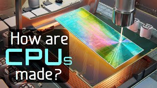
The era of atomic scale engineering presents an unprecedented challenge to making the most advanced technology. The creation of state-of-the-art semiconductor devices rely on etch and deposition processes. Explore career opportunities at Lam Research: https://bit.ly/48cqg0g
Lam Research website: https://www.lamresearch.com/
LinkedIn: / lam-research
Facebook: / lamresearchcorporation
X: / lamresearch
Instagram: / lam.research
Atomic layer etch and deposition help create the most advanced semiconductor structures even with high aspect ratios or 3-dimensional geometries. Multi-step processes happen fast by using plasma and switching between absorption and desorption to fine tune material.
show more